MOCVD System
Example of Crystal Growth Data
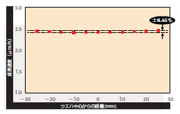
Uniformity of Crystal Film Thickness
The uniformity of crystals formed on the substrate is affected by the uniformity of reactor shape and substrate heating. The uniformity of film thickness is ±0.65% on the Φ2" substrate. (Refer to a graph below.)
|
|
Crystal Purity
The purity of crystals is affected by the airtightness of devices and the device configuring materials. We have used the materials with less degasification for members for heater and so on to prevent contamination. A result of hole measurement of non-dope GaAs crystals at the liquid nitrogen temperature (77K) is as follows:
- Carrier electron density: 1.91×10⁻¹³cm-3
- Carrier mobility: 134,000cm2cm /V.S
Thus, high purity crystal films are formed.
|
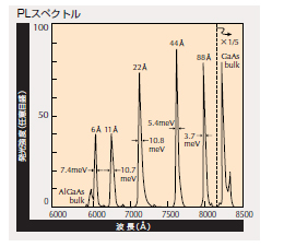
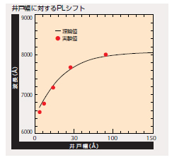
Heterointerface Steepness
In order to reduce sagging on the boundary surface of different kinds of crystals, it is necessary to have a structure without gas accumulation and a precise gas control technique. In a single quantum well (SQW) structure on the GaAs substrate, the steepness of hetero interface is evaluated.
A transmission electron microscopy (TEM) photography shows the crystals of 6Å, 11Å, 22Å, 44Å, and 88Åin thickness, which are clipped by AlGaAs crystals of 500Åin thickness. In addition, an amount of peak shift according to PhotoLuminescence (PL) evaluation coincides with a theoretical value that is determined from a quantum effect, thus it is known that a hetero interface is in a good state.
|
PL spectrum |
PL shift for well width |